

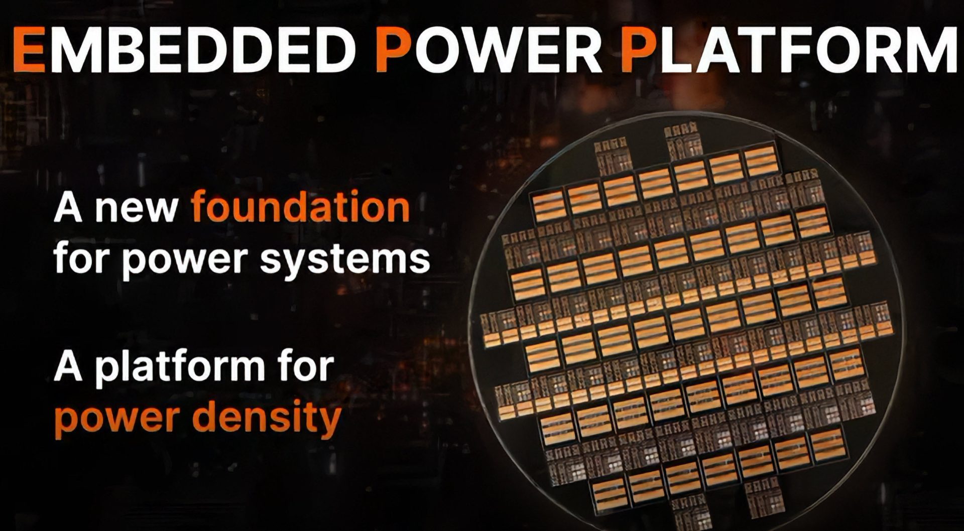
Onsemi is working on an Embedded Power Platform, or EPP, that replaces the traditional printed circuit board (PCB) substrate with a silicon wafer. The company aims to use the approach to make chips more efficient and achieve up to 5x higher power density for artificial intelligence (AI) chips and electric vehicles (EVs), according to Wccftech.
Power modules are currently placed within the PCB. As advanced packaging develops, power systems are increasingly being embedded within the package substrate. Onsemi’s EPP is intended to extend that direction by using silicon wafers as part of the power platform.
Wccftech cites Intel’s EMIB as an example of advanced packaging. In that design, through-silicon vias (TSVs) route power to the chip around the embedded package. Intel’s EMIB-T takes the concept further by routing power through the embedded package.
Onsemi’s proposal is focused on improving power efficiency and density for demanding chip applications. The company is still working on the EPP solution, and the supplied source does not provide a release date or specific product list.
Comments
0No comments yet. Be the first to comment.