

SK Hynix is developing solid-state drive (SSD) controllers with more than 100 compact processors to handle data transfers. The company says its Hynix Transaction Processing Unit (H-TPU) architecture reduces processor power needs and chip area.
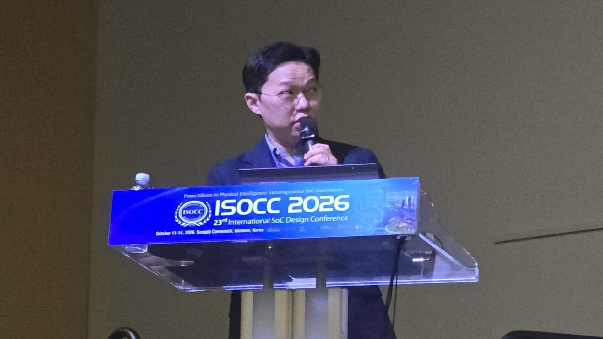
At the International SoC Design Conference, SK Hynix vice president Koo In-je said general-purpose CPUs in SSD controllers are reaching limits in power consumption and area. H-TPUs are designed to handle common input/output (I/O) paths, including routine data reads and writes, metadata updates and buffer control. Conventional CPU cores would remain responsible for more complex work, such as error recovery and storage policy decisions.
SK Hynix says each H-TPU uses 4% of the chip area occupied by a general-purpose CPU core and about 2.5% of its power. The controller activates units needed for each request and idles the others. The architecture uses a four-stage pipeline and sequential execution.
The company plans to use H-TPUs in upcoming enterprise SSD controllers and its Storage Next architecture, which targets smaller data requests from newer AI models, including transactions of 512 bytes or less—one-eighth of a conventional 4KB data unit. SK Hynix also plans to pair the technology with High Bandwidth Flash (HBF), which is expected to reach the market next year, and extend it to its AIN storage portfolio: AIN P, AIN B and AIN D.
SK Hynix has not said when H-TPUs will appear in specific commercial products or quantified their effect on overall SSD performance.
Comments
0No comments yet. Be the first to comment.