

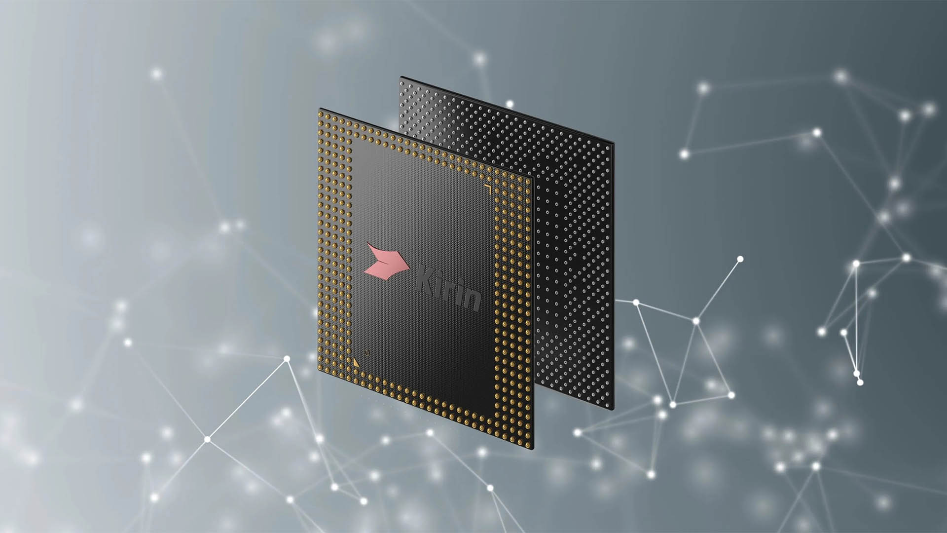
New die shots of Huawei’s Kirin 9050 Pro show two dies bonded together: a compute-focused logic die and an SRAM die.
Kurnal Insights published the images. The source article says the logic die is made on SMIC’s N+3 process, while the SRAM die uses the N+2 process. It describes the bonding method as LogicFolding.
The arrangement combines compute logic with cache memory and SRAM in a two-die package. The images show the chip’s dies, but the source provides no measurements of the package or evidence quantifying any reduction in its footprint.
The source presents the design as an example of Huawei using LogicFolding to reduce chip footprint. The die shots support the description of the two bonded dies and their stated process nodes; they do not independently establish the technique’s broader viability.
Comments
0No comments yet. Be the first to comment.