

Intel has produced its 1 millionth test wafer for high-NA EUV lithography, according to Wccftech. The milestone is presented as evidence that Intel has moved 2-4 years ahead of Samsung and TSMC in the technology.
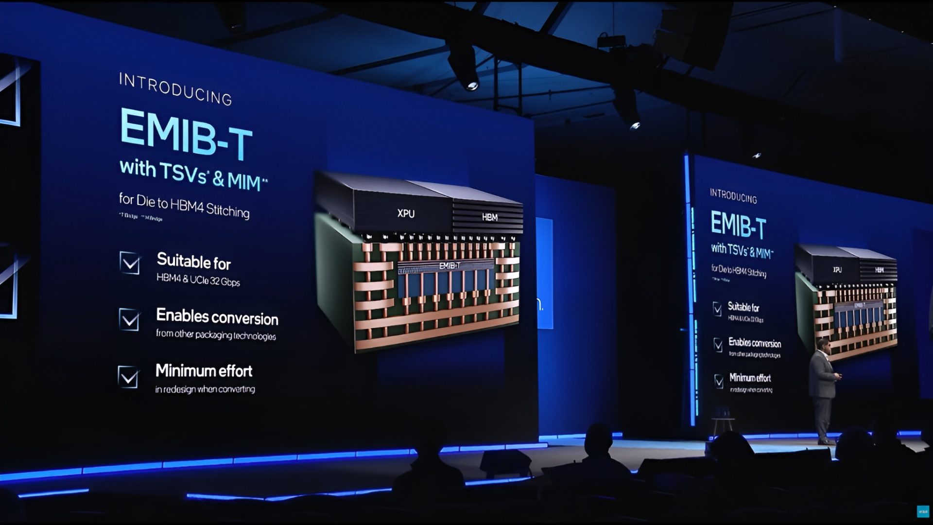
The report also highlights Intel's expanding EMIB-T advanced-packaging capacity. UBS believes Intel can meet MediaTek's growing TPU-related demand for EMIB-T and package over 2 million substrates by 2028.
UBS's assessment links the opportunity to Intel's execution strategy and yields on EMIB-T. The report says the wider industry is becoming increasingly optimistic about Intel's position in advanced packaging.
Intel's progress in high-NA EUV and EMIB-T reflects two separate parts of its manufacturing strategy: lithography technology and advanced packaging. The 1 millionth test wafer is associated with high-NA EUV, while the capacity forecast concerns EMIB-T substrates and MediaTek's TPU-related demand.
The available report does not provide additional details about the test wafer's production process, the identity of the packaged products, or the financial value of the potential business. Its central claims are Intel's reported high-NA EUV lead, the 1 millionth test wafer milestone, UBS's EMIB-T assessment, and the projection of over 2 million substrates by 2028.
Comments
0No comments yet. Be the first to comment.