

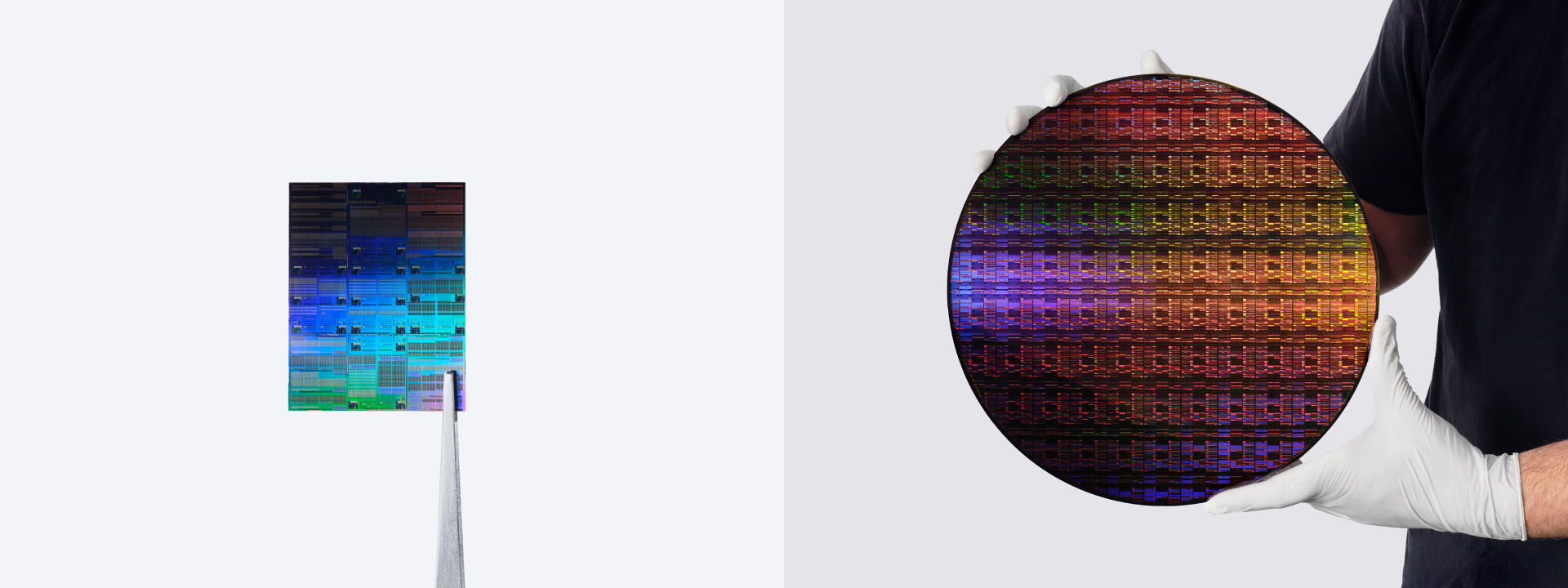
IBM plans to make process development kits (PDKs) for its 0.7-nanometer Nanostack technology available to chip designers in the first quarter of 2027, according to Wccftech. The kits are intended to let interested designers familiarize themselves with the process.
Wccftech reports that IBM launched the 0.7-nanometer technology in June. The report describes Nanostack as an extension of existing chip manufacturing technologies and says the approach seeks to improve compute and memory chips.
The article identifies 2-nanometer manufacturing as the latest chip process currently in mass production. It presents the upcoming PDK availability as an opportunity for chip firms to explore IBM’s technology ahead of wider adoption. The report does not provide further details about the kits or a timeline for broader use.
Comments
0No comments yet. Be the first to comment.